- 您现在的位置:买卖IC网 > Sheet目录39249 > LM4882MM/NOPB (NATIONAL SEMICONDUCTOR CORP) 0.48 W, 1 CHANNEL, AUDIO AMPLIFIER, PDSO8
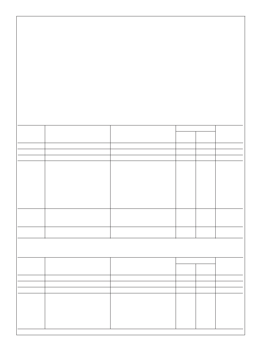
Absolute Maximum Ratings (Note 1)
If Military/Aerospace specified devices are required,
please contact the National Semiconductor Sales Office/
Distributors for availability and specifications.
Supply Voltage
6.0 V
Storage Temperature
65C to +150C
Input Voltage
0.3V to V
DD + 0.3V
Power Dissipation (Note 3)
Internally limited
ESD Susceptibility (Note 4)
2000V
PIn 5
1500V
Junction Temperature
150C
Soldering Information
Small Outline Package
Vapor Phase (60 seconds)
215C
Infrared (15 seconds)
220C
See AN-450 "Surface Mounting and their Effects on
Product Reliability" for other methods of soldering surface
mount devices.
Thermal Resistance
θ
JC (MSOP)
56C/W
θ
JA (MSOP)
210C/W
θ
JC (SOP)
35C/W
θ
JA (SOP)
170C/W
Operating Ratings
Temperature Range
T
MIN
≤ T
A
≤ T
MAX
40C
≤ T
A
≤ 85C
Supply Voltage
2.4V
≤ V
DD
≤ 5.5V
Electrical Characteristics (Notes 1, 2)
The following specifications apply for V
DD = 5V unless otherwise specified. Limits apply for TA = 25C.
Symbol
Parameter
Conditions
LM4882
Units
(Limits)
Typical
Limit
I
DD
Quiescent Current
V
IN = 0V, IO = 0A
2
4.0
mA (max)
I
SD
Shutdown Current
V
pin1 =VDD
0.5
5
A (max)
V
OS
Offset Voltage
V
IN = 0V
5
50
mV (max)
P
O
Output Power
THD+N=1% (max);f=1 kHz;
R
L =4
380
mW
R
L =8
270
250
mW (min)
R
L =32
95
mW
THD+N= 10%;f=1kHz
R
L =4
480
mW
R
L =8
325
mW
R
L =32
125
mW
THD + N
Total Harmonic Distortion + Noise
R
L =8
,P
O = 250 mWrms;
0.5
%
R
L =32
,P
O = 85 mWrms;
0.1
%
f=1kHz
PSRR
Power Supply Rejection Ratio
V
pin3 = 2.5V, V ripple = 200 mVrms,
f = 120 Hz
50
dB
Electrical Characteristics (Notes 1, 2)
The following specifications apply for V
DD = 3V unless otherwise specified. Limits apply for TA = 25C.
Symbol
Parameter
Conditions
LM4882
Units
(Limits)
Typical
Limit
I
DD
Quiescent Current
V
IN = 0V, IO = 0A
1.2
mA
I
SD
Shutdown Current
V
pin1 =VDD
0.3
A
V
OS
Offset Voltage
V
IN =0V
5
mV
P
O
Output Power
THD+N=1% (max);f=1kHz
R
L =8
80
mW
R
L =32
30
mW
THD+N= 10%;f=1kHz
R
L =8
105
mW
R
L =32
40
mW
LM4882
www.national.com
3
发布紧急采购,3分钟左右您将得到回复。
相关PDF资料
LM4882M/NOPB
0.48 W, 1 CHANNEL, AUDIO AMPLIFIER, PDSO8
LM556ICN
DUAL PULSE; RECTANGULAR, TIMER, PDIP14
LM5756
3.5 A SWITCHING REGULATOR, 100 kHz SWITCHING FREQ-MAX, ZFM5
LM7001JM
PLL FREQUENCY SYNTHESIZER, 130 MHz, PDSO20
LM7001M
PLL FREQUENCY SYNTHESIZER, 130 MHz, PDSO20
LM7006
PLL FREQUENCY SYNTHESIZER, 400 MHz, PDIP20
LM7006H
PLL FREQUENCY SYNTHESIZER, 400 MHz, PDIP20
LM7007M
PLL FREQUENCY SYNTHESIZER, 520 MHz, PDSO24
相关代理商/技术参数
LM4882MX/NOPB
制造商:Texas Instruments 功能描述:Audio Amp Speaker 1-CH Mono 0.48W Class-AB 8-Pin SOIC N T/R
LM4883
制造商:NSC 制造商全称:National Semiconductor 功能描述:Dual 2.1W Audio Amplifier Plus Stereo Headphone
LM4883A E WAF
制造商:Texas Instruments 功能描述:
LM4883SQ
制造商:NSC 制造商全称:National Semiconductor 功能描述:Dual 2.1W Audio Amplifier Plus Stereo Headphone
LM4883SQ/NOPB
功能描述:IC AMP AUDIO PWR 3W STER 24LLP RoHS:是 类别:集成电路 (IC) >> 线性 - 音頻放大器 系列:Boomer® 产品培训模块:Lead (SnPb) Finish for COTS
Obsolescence Mitigation Program 标准包装:2,500 系列:DirectDrive® 类型:H 类 输出类型:耳机,2-通道(立体声) 在某负载时最大输出功率 x 通道数量:35mW x 2 @ 16 欧姆 电源电压:1.62 V ~ 1.98 V 特点:I²C,麦克风,静音,短路保护,音量控制 安装类型:表面贴装 供应商设备封装:25-WLP(2.09x2.09) 封装/外壳:25-WFBGA,WLCSP 包装:带卷 (TR)
LM4883-SQ_BOM-001A
制造商:NSC 制造商全称:National Semiconductor 功能描述:Demo Board
LM4883SQX/NOPB
功能描述:IC AMP AUDIO PWR 3W STER 24LLP RoHS:是 类别:集成电路 (IC) >> 线性 - 音頻放大器 系列:Boomer® 产品培训模块:Lead (SnPb) Finish for COTS
Obsolescence Mitigation Program 标准包装:2,500 系列:DirectDrive® 类型:H 类 输出类型:耳机,2-通道(立体声) 在某负载时最大输出功率 x 通道数量:35mW x 2 @ 16 欧姆 电源电压:1.62 V ~ 1.98 V 特点:I²C,麦克风,静音,短路保护,音量控制 安装类型:表面贴装 供应商设备封装:25-WLP(2.09x2.09) 封装/外壳:25-WFBGA,WLCSP 包装:带卷 (TR)
LM4884
制造商:NSC 制造商全称:National Semiconductor 功能描述:2.1W Differential Input, BTL Output Stereo Audio Amplifier with RF Suppression and Shutdown